
LABORATORY FOR NEW DETECTORS AND ESTABLISHMENT OF INTELLIGENT PROCESS CONTROL SYSTEMS
PROJECT BG05M2OP001-1.001-0008 | NATIONAL CENTER OF MECHATRONICS AND CLEAN TECHNOLOGIES
Managers:
Prof. Dr. Evgenia Valcheva (Sofia University St. Kliment Ohridski)
e-mail: epv@phys.uni-sofia.bg
phone 02 8161 843
Assoc. Prof. Dr. Veselin Donchev (Sofia University St. Kliment Ohridski)
e-mail: vtd@phys.uni-sofia.bg
phone 02 8161 701
The Laboratory studies semiconductor nanostructures and bulk materials for optoelectronic and photovoltaic applications. Semiconductor nanostructures (quantum wells, superlattices, quantum wires, quantum dots) for optoelectronic applications are being studied by spectroscopic methods, namely LED light emitters, infrared detectors, optical memories, photovoltaic elements, highly efficient semiconductor components – and nanoelectronics based on quantum effects. The studied objects and systems are components of modern mechatronic devices.
ACTIVITIES
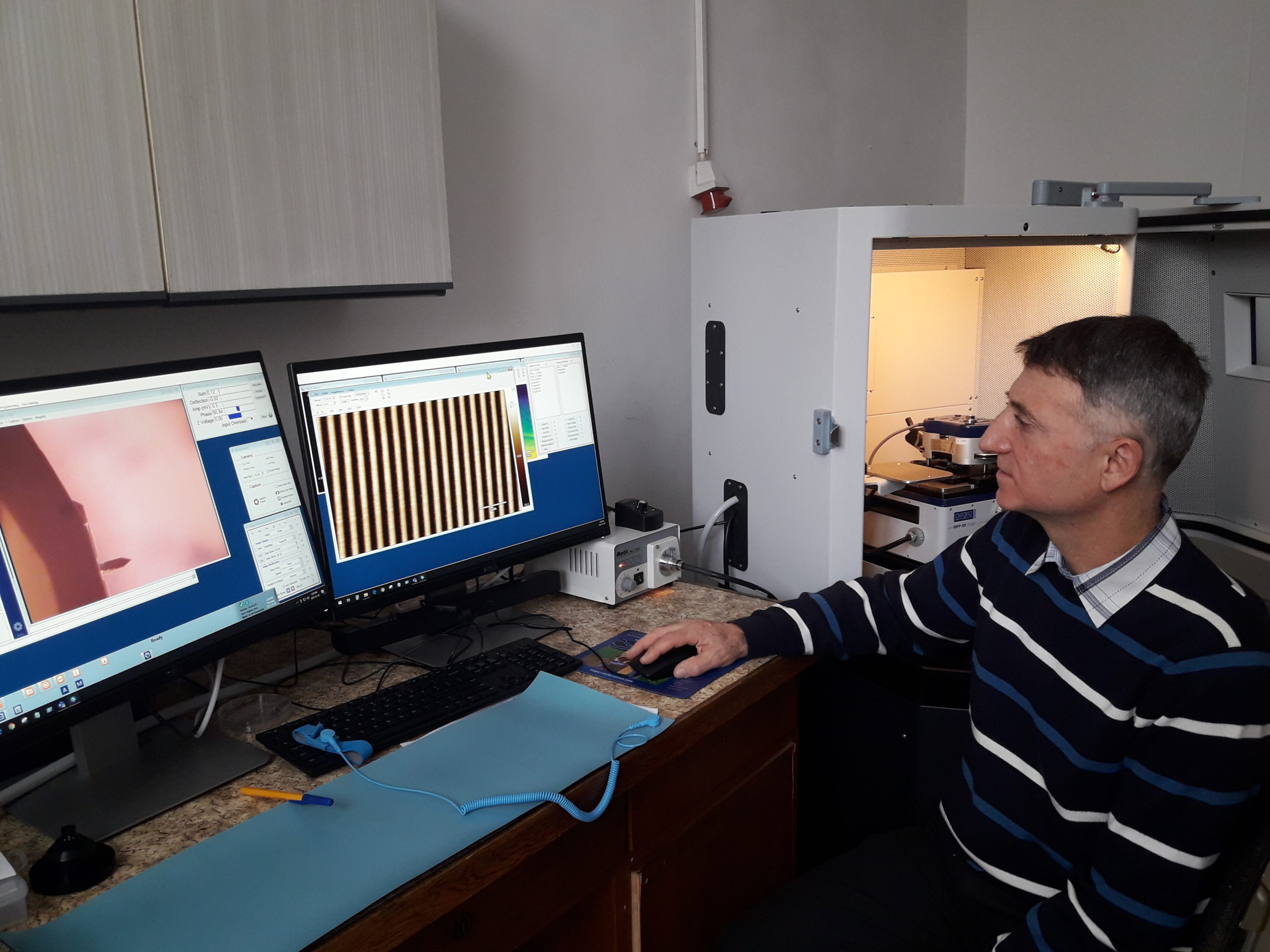
The microscope is used to study a wide range of modern materials – thin films and coatings for sensors, detectors, photovoltaics, media and more. The dimensions of these films and the structures made of them (thickness, relief, grain sizes and domains, etc.) set an important condition for their characterization at resolutions below nanometers to micrometers, which is possible with the installed AFM.
The use of AFM 3D Origin provides information that is critical in the development, optimization of thin films and the monitoring of their growth processes, as well as in the rationalization of design paths to achieve the desired functional properties of mechatronics instruments.
SERVICES
- Research of a wide range of modern materials - thin films and coatings for sensors, detectors, photovoltaics, media, etc.
- Investigation of the optical properties of photovoltaic structures
- Examination of graphene and graphene-like carbon materials by atomic force microscopy
- Study of conductivity properties
- Topography of microobjects
EQUIPMENT
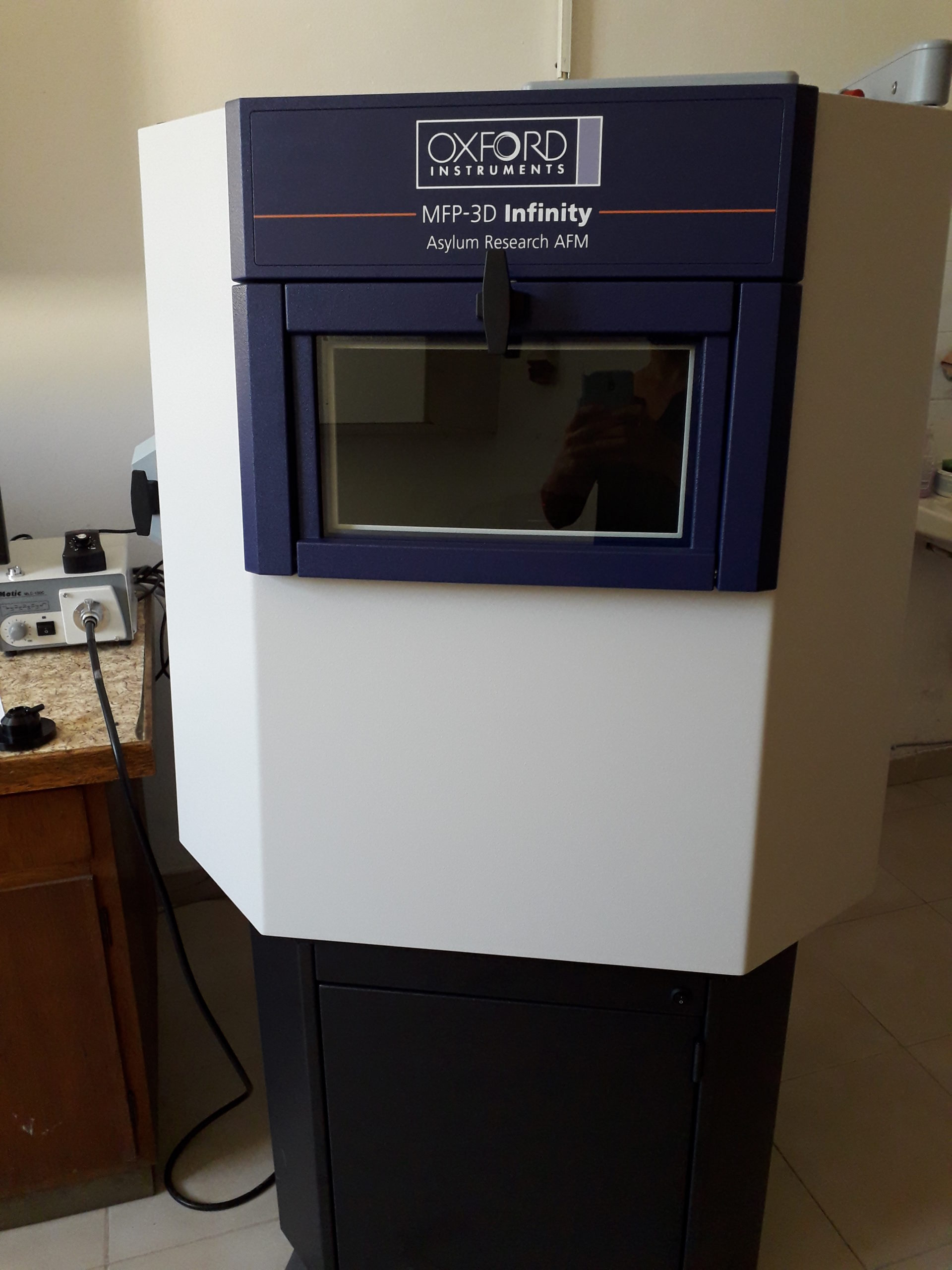
The MFP-3D Origin Atomic Power Microscope (AFM) is the leading member of the MFP-3D AFM family. It has the widest range of image modes and characterization accessories, with flexibility, powerful features and a system architecture that allows for future expansion. The following modes are included: AFM contact mode, tapping mode, Kelvin Probe Force Microscopy (KPFM), Magnetic Force Microscopy (MFM), Conductive AFM, Nanolithography, Nanomanipulation, Scanning Tunneling Microscopy (STM).